REVIEW ● OPEN ACCESSRead More
1. Introduction
With the ever-growing demands for soft deformable sensors and devices, the integration of electronic systems on 3D curvilinear surfaces starts to gain momentum in various applications i.e., bio-integrated devices, health monitoring of structures, and 3D multifunctional electronics. Challenges of fabricating and integrating them on 3D complex shapes or the soft, hierarchically structured, and even dynamically changing surfaces raise up. Efforts to address these challenges lead to rapid development of various stretchable structures with advanced manufacturing techniques to integrate the devices on the 3D curvilinear surfaces. The exploration of novel nanomaterials and their composites further expands the functionality and capability of the resulting devices. The stretchable structures and functional nanomaterials for conformal electronics have been extensively discussed in many reviews, while the comprehensive survey of conformal fabrication techniques on complex surfaces is still highly desirable.
Wanqing Zhang, Dr. Ling Zhang, Prof. Yabin Liao and Prof. Huanyu Cheng, from The Pennsylvania State University, wrote a review ‘Conformal manufacturing of soft deformable sensors on the curved surface’ on IJEM. In this article, the authors provide a comprehensive summary that includes various advanced transfer printing and direct conformal printing techniques, followed with applications to fabricate sensors and devices in conformal manufacturing. Next, recent advances in conformal electronics are discussed. In the end, the authors highlight the existing challenges and a small fraction of opportunities for future development of conformal manufacturing. Figure 1 shows the recent advancement of conformal manufacturing of soft deformable devices on curved surfaces.
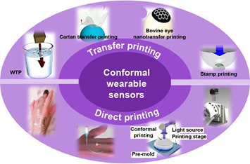
Figure 1. Conformal manufacturing of soft deformable sensors on curved surfaces.Combined with stretchable structures and functional nanomaterials, various transfer printing (reproduced with permission from ref. 71-74) and direct printing/writing techniques (reproduced with permission from ref. 17, 75-77) are capable of integrating conformal sensors/devices on 3D curvilinear and even dynamically changing surfaces.
2. Background
Diverse fabrication methods i.e., contact printing, nanoimprint lithography and beam lithography have been widely used to fabricate sensors and electronics on 2D planar substrates. But these representative inherently planar methods are not directly suitable to manufacture conformal devices on 3D curved surfaces due to the limitation in planar fabrication. To address the challenge, various stretchable structures, and novel nanomaterials as well as their composites are explored. The commonly used stretchable structures for conformal electronics include wavy geometries, strain isolation, filamentary serpentine or mesh designs, helical coils, and origami/kirigami. Combining with stretchable structures and the use of advanced transfer printing techniques, planar fabrication methods can manufacture conformal devices on complex surfaces. The widely used nanomaterials include metal nanowires, carbon nanotubes, graphene, liquid metal alloy, organic films. Combining with functional nanomaterials, various direct printing and writing methods are also developed to fabricate conformal electronics on curved surfaces with intimate contact even over a large area.
3. Recent advances
Recent advances in conformal manufacturing of soft deformable sensors and devices on curved surfaces have been divided into three sections: transfer printing techniques, direct printing technique and advanced writing methods. Representative fabrication methods and their applications are discussed in each section.
Advanced transfer printing techniques
Transfer printing enables planar fabrication methods to manufacture conformal devices on complex surfaces by integrating micro/nanoscale thin film devices prepared on a planar growth substrate on to surface of the target substrate. These techniques have simple process with a relatively high yield. Figure 2 shows the stamp-based printing, figure 3 shows the Cartan transfer printing, figure 4 shows the adhesive-based nanotransfer printing and figure 5 shows the water transfer printing.
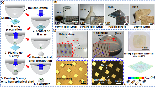
Figure 2. Additive stamp printing with a pneumatically inflated elastomeric balloon as a conformal stamp to fabricate various 3D curvy electronics, reproduced with permission from ref.71. (a) Schematic to show the use of a pneumatically inflated elastomeric balloon as a conformal additive stamp. (b) The serpentine metal mesh on convex edge, concave edge, pyramid, and uneven surfaces. (c) The retrieved 39 x 39 Si pellet array (each pellet of 100 x 100 µm) on a balloon stamp and printed on a hemispherical shell, with high yield (>99%) and small strain (0.01%) in all the Si pellets.
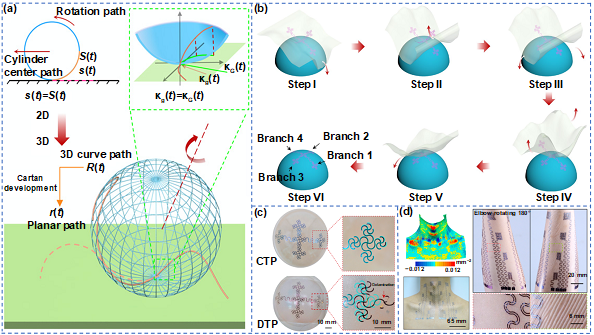
Figure 3. Cartan transfer printing (CTP) to transfer large-area tattoo-like electrodes from a bendable cloth donor substrate to the non-developable neck skin region, reproduced with permission from ref.72.(a) Schematic of the CTP and (b) its step-by-step processes. (c) Patterns transfer printed by CTP and direct transfer printing (DTP). (d) large-area tattoo-like electrodes laminated on the neck through CTP with Gaussian curvature map of the neck, and large-area epidermal electrodes with/without substrate attached on forearm under 180-degree rotation.
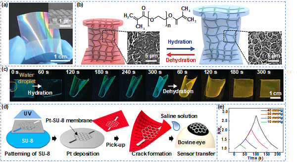
Figure 4. Nanotransfer printing with a smart hydrogel adhesive to fabricate a nanoscale crack sensor onto a bovine eye for detecting intraocular pressure, reproduced with permission from ref.73. (a) The fabricated wet-responsive and reconfigurable poly(ethylene glycol) dimethacrylate (PEGDMA) adhesive, where the inset is an SEM image of the PEGDMA nanostructure array of the adhesive. (b) The reversible hydration and dehydration processes of the PEGDMA array. (c) The hydration-induced spontaneous bending of the PEGDMA adhesive film and re-flattening of the adhesive during dehydration. (d) The fabrication of the nanoscale crack sensor and its subsequent transfer printing onto a bovine eye using the PEGDMA adhesive with saline solution. (e) Normalized resistance variation showing the reversible loading-unloading behavior at different pressures.
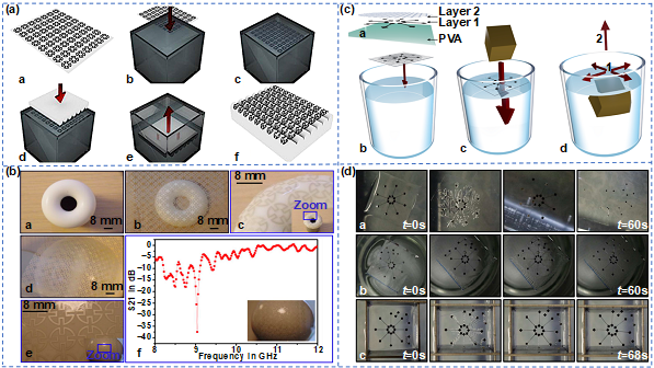
Figure 5. Water transfer printing.(a) Water transfer printing to fabricate an array of frequency selective surface (FSS) metallic pattern layers on curved dielectric surfaces. (b) The fabricated 3D FSS on the complex structures, including a donut-shaped object and a semi-spherical object. (a) and (b) reproduced with permission from ref. 74 (c) Adapted water transfer printing with rigid film guides on the edges of the substrate to avoid folds. (d) PVA dissolution behavior with unlined aluminum patterns designed in a star configuration. When the PVA is dissolved, each line composing the star can move and the pattern is deformed (top). When an additional layer of SU8 is printed on aluminum and designed in a square mesh configuration, lines cannot move and the patterns are not deformed (middle). Due to the additional added film guides in the periphery of the PVA substrate, radial forces are drastically reduced to ensure pattern accuracy (bottom). (c-d) reproduced with permission from ref. 106.
Direct conformal printing techniques
Compared to transfer printing with limited efficiency due to multiple transfer steps and unavoidable distortion during fabrication process, various direct printing techniques are introduced as an effective alternative to address these challenges. Figure 6 shows the five-axis printing systems, figure 7 shows the electrodynamic direct printing, and figure 8 shows the direct printing using stereolithography.
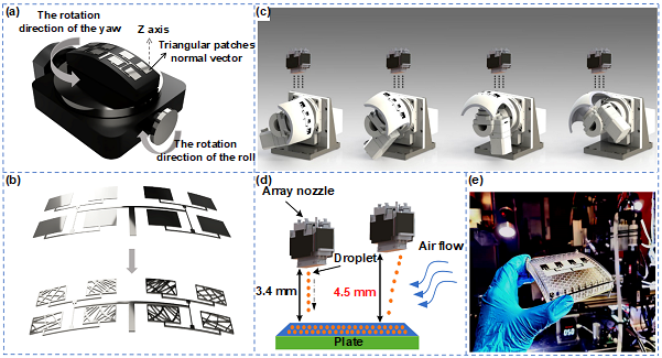
Figure 6. Five-axis printing systems for conformal microstrip antenna fabrication.(a) Schematic of a five-axis printing system. (b) The conversion of the 3D surface into a polarity of 2D triangular patches. (c) Five-axis inkjet printing system with arrayed nozzles. (d) A schematic to show the air drift from the airflow. (e) The fabricated conformal microstrip antenna array with four units. (c-e) reproduced with permission from ref. 75.
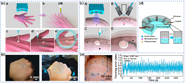
Figure 7. Direct printing on freely moving objects in real-time.(a) A hybrid manufacturing process that combines surface-mounted electronic components with directly printed electrical interconnects on freely moving hands. (b) Fiducial markers placed around the automatically pick-and-placed LED on a human hand (left). The adaptive 3D printing of the wireless device on a human hand that can move freely in the workspace (right). (a) and (b) reproduced with permission from ref. 76 (c) An in-situ 3D printing system to directly fabricate an electrical impedance tomography (EIT) sensor. (d) The layered design of the hydrogel-based EIT sensor. (e) In situ 3D printing of hydrogel ink on a porcine lung, with the tracking error as a function of time (mean of 0.657 mm). (c-e) reproduced with permission from ref. 128.
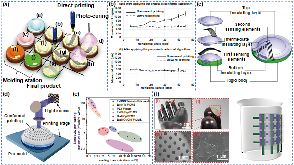
Figure 8. Direct printing using stereolithography. (a) Conformal direct printing with soft modeling for fabricating stretchable multi-layered tactile piezoresistive sensors on freeform surfaces. (b) Filament width variations in upward and downward printing before (top) and after (bottom) applying a conformal printing algorithm. (c) The proposed mechanically compliant, conformal, and multilayered tactile sensor. (a-c) reproduced with permission from ref. 129. (d) Conformal 3D printing based on projection stereolithography. (e) Comparison of relative sensitivity between the chemically functionalized BNNTs-based composite and other piezoelectric/polymer composites. (f) The left shows a printed conformal device on the fingertip of a rubber hand model with SEM images of the device surfaces and chemically functionalized BNNTs/resin composite. The right shows the tactile sensor array of 44 on the curved surface of a beaker to capture force distribution. (d-f) reproduced with permission from ref. 77.
Other advanced fabrication methods
In addition to transfer printing and direct printing methods, other fabrication methods include spray coating and draw-on-skin electronics. These advanced conformal manufacturing techniques enhance interfacial adhesion and can easy operation. Figure 9 shows the fabrication of draw-on-skin electronics using novel writing tools, and figure 10 shows the direct sensor fabrication on skin using a novel sintering aid layer.
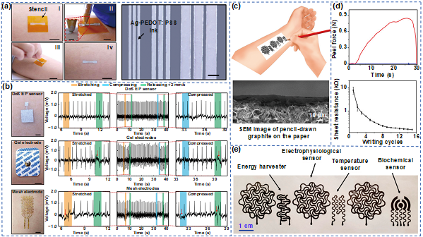
Figure 9. Fabrication of draw-on-skin electronics.(a) Draw-on-skin electronics with functional inks. The line width of the Ag-PEDOT:PSS ink can be controlled by varying the pen tip diameter, where the line widths are 0.3 mm, 0.5 mm, and 1 mm from left to right. (b) DoS EP sensors, gel electrodes, and mesh electrodes with ECG signal recorded upon the skin deformation. (a) and (b) reproduced with permission from ref. 136 (c) Draw-on-skin electronics by using a 9B sketching pencil on office copy papers. (d) Peel-adhesion test of pristine papers (blue) and papers with spray-coated Silbione (red) on the human forearm, where the stickiness of the resulting on-skin electronic devices can be drastically improved from ~0.01 to ~0.85 N after Silbione coating (top). The sheet resistance of the pencil-drawn graphite on papers reduces from ~10 kΩ sq-1 to 160 Ω sq-1 as the writing cycle increases from the 1st to 15th cycle (bottom). (e) Pencil-paper on-skin bioelectronic devices. (c-e) reproduced with permission from ref. 139
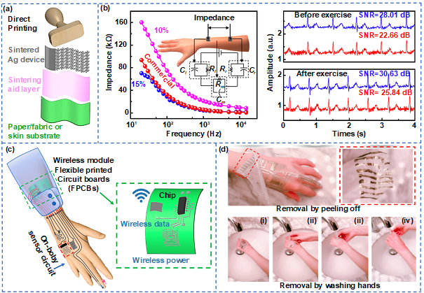
Figure 10. Direct sensor fabrication on the skin, reproduced with permission from ref. 17. (a) The simple process of preparing the directly printed on-body sensors sintered at room temperature. (b) Impedance measurements as a function of frequency from two Ag electrodes of the same size separated by a given distance of 10 cm directly printed and room temperature-sintered on the human skin (left). ECG signals collected using the Ag electrodes on the sintering aid layer with 15 wt% PVA paste (blue) with a larger SNR than those from the commercial electrodes (red) (right). (c) The soft body area sensor network consisting of various on-body sensors (e.g., electrodes and temperature/hydration sensors) and an FPCB. (d) The on-body sensing film can be conveniently removed with negligible effects on the skin by peeling off (top) or washing hands in warm water flow (bottom).
4. Perspectives
From the recent advances and achievements of conformal electronics on complex 3D surfaces, it is worth noting that challenges still exist to represent a small fraction for future development in this burgeoning field. Although it is still challenging to correlate the designed pattern on the 2D surface with that on the curved surface during transfer printing, the computing framework based on the topology method and conformal mapping theory for free-form periodic metasurfaces may by explored. Though a variety of ink has been applied for direct printing of conformal electronics, there is still a wide range of nanomaterials that are challenging to use in fabrication and application. In addition, achieving strong and robust adhesion between the soft deformable sensors and the curved surfaces is still challenging. Besides, there is also an opportunity to explore a set of functional degradable materials for conformal transient electronics.
5. About the Authors

Dr. Cheng was appointed an Assistant Professor of Engineering Science and Mechanics (ESM) and as a member of the Materials Research Institute (MRI) at The Pennsylvania State University in August 2015, and was awarded the Dorothy Quiggle Career Development Professorship in September 2015. He has been affiliated with the Penn State Institutes of Energy and the Environment since November 2015, the Institute for Computational and Data Sciences (ICDS) since June 2017, the Center for Research on Advanced Fiber Technologies since September 2017, the Center for Biodevices since February 2020, the Engineering, Energy, & Environmental Institute (E3I) since March 2020, the Sustainability Institute since April 2020, and the Planetary System Science Center (PSSC) since April 2021. He has served as an advisor for the Schreyer Honors College since August 2015, on the Intercollege Graduate Degree Program in Materials Science and Engineering since February 2016, as the Graduate Faculty in Mechanical Engineering since January 2021, an Affiliate Assistant Professor in Biomedical Engineering since February 2021, an Affiliate Associate Professor in Architectural Engineering since May 2021, and a Graduate Faculty in Additive Manufacturing and Design since June 2021. His interdisciplinary research links materials, mechanical, electrical, and biomedical engineering with the life sciences and medicine, through the development of new stretchable and conformable, wearable, electronic sensing, device technolog. Working with his students and collaborators, Dr. Cheng has published over 50 journal papers and 5 book chapters since joining Penn State, bringing his total to over 100 journal papers, with total citations of 12,879 and an H-index of 45 according to Google Scholar. While at Penn State, his research has earned him numerous awards, including: the Global Young Academy for scientists under age 40 in 2016; Forbes 30 under 30 Science category in 2017; 1st place in the PA Ben Franklin TechCelerator program in 2020; 70th Lindau Nobel Laureate Meeting in 2020; 2021 Scialog Fellow; 2021 TMS Frontiers of Materials Award; Panel Fellow in the NSF CMMI Game Changer Academies for Advancing Research Innovation; Invitee to the 4th World Laureates Forum in 2021; Invited Participant to the eighth Arab-American Frontiers of Science, Engineering, and Medicine Symposium by the U.S. National Academy of Sciences; and a finalist for the Falling Walls Science Breakthroughs of the Year 2021 in Engineering and Technology.


